The EB Mask Writer is a device that integrates advanced elemental technologies such as precision machine control, large-scale data processing, and laser measurement technology, with electron beam writing control technology as the core technology.
Features
Key Technologies
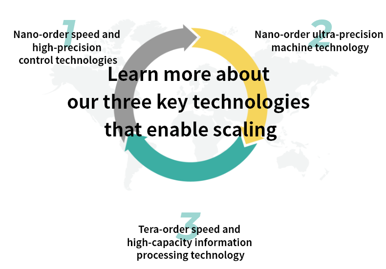
From nano to tera
Electron beam mask writers are systems based on technologies from a number of diverse areas, including physics, chemistry, electrical engineering, mechanical engineering, control engineering, information processing engineering, and metrology.
“Electron beam mask writers are a composite of technologies where various leading-edge specialties merge. These range from minute geometry, typified by nanotechnology (at the scale of one billion to one), to technology for processing enormous amounts of data on the "tera" (one trillion) scale. Driven by a commitment to challenge new frontiers and inspired by the slogan "endlessly challenging," we are working to realize our aspirations and contribute to the advancement of the semiconductor industry, our society, and humankind.
Nano-order speed and high-precision control technologies
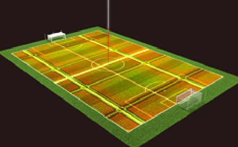
Lining up one yen coins into a soccer field in just two seconds ! High speed and high-precision control technologies
High speed and high-precision control technologies As the same principle of a TV cathode ray tube, electron beam mask writers use electrons emitted electrons from an electron gun to form a circuit pattern on photomask. Electron beam mask writers precisely position the electrons to write complex circuit patterns on the photomask with an accuracy of a nanometer-order scale.
This speed and precision of positioning is comparable to lining up 20mm-diameter one yen coins into a soccer field within an error margin of 0.2mm, under just 2 seconds without missing a single coin. Only our high-speed, high-precision control technologies, enable us to produce a mask writer capable of writing high-quality semiconductor circuit patterns with high throughput.
Nano-order ultra-precision machine technology
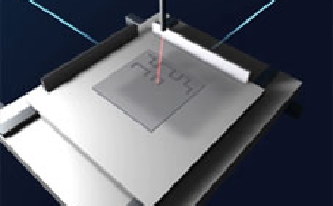
The ultimate image stabilizer ! Nanometer-order ultra-precision machine technology
Electron beam mask writers have the photomask placed on a stage that moves within a plane, and write the circuit patterns while continually moving the stage. The stage is feedback-controlled using positional information from a precision sensor known as a laser interferometer. Moving the stage that has several tens of kilograms causes mechanical vibrations. There are mainly two types of mechanical vibrations: relatively low frequency vibrations that can be suppressed by mechanical controls, and high frequency vibrations that are difficult to track mechanically. Both of these vibrations need to be controlled in the electron beam mask writers to maintain the pattern position accuracy. To meet these requirements, we have developed and succeeded in applying 1) the highest level ultra-precision stage and optimal mechanical control technology to suppress the relatively low frequency vibrations to a sub-nanometer level, and 2) a beam tracking technology that feeds back signals from the laser interferometer to the electron beam deflection controls to suppress the high frequency vibrations to a sub-nanometer level. By combining these two technologies, the stage position in relation to the electron beam is controlled to be almost stationary to the sub-nanometer level, much like an image stabilizer.
Tera-order speed and high-capacity information processing technology
The ultimate reliability technology !? Tera-order, high-capacity information processing technology
Tera-order speed and high-capacity information processing technology With the scaling of semiconductors, processor and memory performance has improved dramatically and computer processing power has increased exponentially. As semiconductor integration precision improves, the circuit pattern writing data handled by electron beam mask writers is becoming enormous. Another factor in the burgeoning amount of data being processed is compensatory information to prevent mutual interference among the labyrinths of patterns. When generating writing data from LSI circuit pattern data, the volume of information can reach the terabyte level (tera = 1,000,000,000,000). NuFlare Technology uses cutting-edge processors to parallel process large volumes of terabyte-class data, and we are developing and implementing high-speed computing technologies.
The volume of figure data needed to describe the circuit patterns is comparable to the data volume of the latest HDD. The electron beam deflection controls can receive all the figure data without a single miss of data order, within just a couple of hours. This means that the electron beam mask writer is required to have the ultimate reliability technology that enables writing one trillion figures without a single error. In the future, data volumes are expected to increase explosively, and we are continuing to develop toward still higher processing speeds.
List of Awards & Papers
List of Awards Received by Nuflare Technology,Inc. Employees
The Okochi Memorial Grand Production Prize(2012)
Date Awarded
March 22th, 2013
Title of Award
The Okochi Memorial Grand Production Prize(2012)
Title of Work
"Development and practical application of electron beam (EB) mask writers."
Organization
Okochi Memorial Foundation
2008 Kanto Region Commendation for Invention, Invention Encouragement Award
Date Awarded
November 5th, 2008
Title of Award
2008 Kanto Region Commendation for Invention, Invention Encouragement Award
Title of Work
"Improved accuracy of electron beam writing by reducing fogging"
Organization
Japan Institute of Invention and Innovation Tokyo Branch
The Commendation for Science and Technology by the Minister of Education, Culture, Sports, Science and Technology (2007) Prize for Science and Technology (Development Category )
Date Awarded
April 17th, 2007
Title of Award
The Commendation for Science and Technology by the Minister of Education, Culture, Sports, Science and Technology (2007) Prize for Science and Technology (Development Category )
Title of Work
"Development of Proximity Effect Correction for Electron Beam Mask Writing System"
Organization
Ministry of Education, Culture, Sports, Science and Technology
The National Commendation for Invention (2006) The Prize of the Minister of Economy Trade and Industry
Date Awarded
June 19th, 2006
Title of Award
The National Commendation for Invention (2006) The Prize of the Minister of Economy Trade and Industry
Title of Work
"Invention of Proximity Effect Correction for Electron Beam Writing System"
Organization
Japan Institute of Invention and Innovation (JIII)
Refereed Papers by Nuflare Technology,Inc. Employees
Recent progress and future of electron multi-beam mask writer
Publication Year
2023
Title of Paper
Recent progress and future of electron multi-beam mask writer
Name of Journal
Japanese Journal of Applied Physics, Vol. 62, SG0803 (2023)
Study on physical model of resit surface charge in multi-beam mask writer and single variable-shape beam wirters
Publication Year
2021
Title of Paper
Study on physical model of resit surface charge in multi-beam mask writer and single variable-shape beam wirters
Name of Journal
Journal of Micro/Nanopatterning, Materials and Metrology, Vol. 20, 041404 (2021)
Multi-beam mask writer MBM-1000
Publication Year
2018
Title of Paper
Multi-beam mask writer MBM-1000
Name of Journal
Journal of Micro/Nanolithography, MEMS,and MOEMS, Vol. 17, 031205 (2018)
Correction of resist heating effect of variable shaped beam mask writer
Publication Year
2016
Title of Paper
Correction of resist heating effect of variable shaped beam mask writer
Name of Journal
Journal of Micro/Nano Lithography, MEMS,and MOEMS, Vol. 15, 021012 (2016)
Proximity effect correction for mask writing taking resist development process into account
Publication Year
2009
Title of Paper
Proximity effect correction for mask writing taking resist development process into account
Name of Journal
Japanese Journal of Applied Physics, Vol.48, 095004 (2009)
EB writing technique with variable shaped beam for 30 nm and below (in Japanese)
Publication Year
2009
Title of Paper
EB writing technique with variable shaped beam for 30 nm and below (in Japanese)
Name of Journal
Journal of the Japan Society for Abrasive Technology, Vol. 53, 340 (2009)
High accuracy correction of critical dimension errors appearing in large-scale integrated circuits fabrication processes:pattern-based model
Publication Year
2009
Title of Paper
High accuracy correction of critical dimension errors appearing in large-scale integrated circuits fabrication processes:pattern-based model
Name of Journal
Japanese Journal of Applied Physics, Vol.48, 046508 (2009)
High accuracy correction of critical dimension errors taking sequence of large-scale integrated circuits fabrication processes into account
Publication Year
2008
Title of Paper
High accuracy correction of critical dimension errors taking sequence of large-scale integrated circuits fabrication processes into account
Name of Journal
Journal of Micro/Nano Lithography, MEMS, and MOEMS, Vol. 7, 043008 (2008)
Accurate correction of critical dimension errors appearing in LSI fabrication processes
Publication Year
2008
Title of Paper
Accurate correction of critical dimension errors appearing in LSI fabrication processes
Name of Journal
Journal of Micro/Nano Lithography, MEMS, and MOEMS, Vol. 7, 023006 (2008)
Global critical dimension correction: I. Fogging effect correction
Publication Year
2007
Title of Paper
Global critical dimension correction: I. Fogging effect correction
Name of Journal
Japanese Journal of Applied Physics, Vol.46, 3359 (2007)
Global critical dimension correction: II
Fogging Effect Correction
Publication Year
2007
Title of Paper
Global critical dimension correction: II
Name of Journal
Japanese Journal of Applied Physics, Vol.46, 3368 (2007)
High-accuracy proximity effect correction for mask writing
Publication Year
2007
Title of Paper
High-accuracy proximity effect correction for mask writing
Name of Journal
Japanese Journal of Applied Physics, Vol.46, 826 (2007)
Book etc
<caption class="Electron Beam Mask Writer Boasting Overwhelming Market Share in the World", "NEDO Web Magazine Practical Application Document", New Energy and Industrial Technology Development Organization
Date
2012
Title
"Electron Beam Mask Writer Boasting Overwhelming Market Share in the World", "NEDO Web Magazine Practical Application Document", New Energy and Industrial Technology Development Organization
Type
Interview article
<caption class="Electron and Ion Beam Handbook (4th Edition)", The Nikkan Kogyo Shinbunsha,Ltd. (partial author)
Date
2021
Title
"Electron and Ion Beam Handbook (4th Edition)", The Nikkan Kogyo Shinbunsha,Ltd. (partial author)
Type
Book
<caption class="Our company's best!", "Vacuum Journal" July 2019 issue, Japan Vacuum Industry Association
Date
2019
Title
"Our company's best!", "Vacuum Journal" July 2019 issue, Japan Vacuum Industry Association
<caption class="How the Tree of Technology Grows - Imaginative Thinking, Technological Innovation - Part 8 "Electron Scattering Phenomena Standing in the Future of LSI - Proximity Effect Correction Achieved by Simplifying Complex Problems", "Erekiteru" , Toshiba Public Relations department
Date
2007-2008
Title
"How the Tree of Technology Grows - Imaginative Thinking, Technological Innovation - Part 8 "Electron Scattering Phenomena Standing in the Future of LSI - Proximity Effect Correction Achieved by Simplifying Complex Problems", "Erekiteru" , Toshiba Public Relations department
Type
Interview article
<caption class=``How to Invention: Listen to National Commendation for Invention Winners 2006 Minister of Economy, Trade and Industry Invention Award Invention of Proximity Effect Correction Technology for Electron Beam Lithography Equipment'', ``Invention'', Japan Institute of Invention and Innovation
Date
2006
Title
``How to Invention: Listen to National Commendation for Invention Winners 2006 Minister of Economy, Trade and Industry Invention Award Invention of Proximity Effect Correction Technology for Electron Beam Lithography Equipment'', ``Invention'', Japan Institute of Invention and Innovation
Type
Interview article
Sub-Half-Micron Lithography for ULSIs
(Cambridge University Press)
Section 4.4 Proximity effect correction
Date
2000
Title
Sub-Half-Micron Lithography for ULSIs
(Cambridge University Press)
Section 4.4 Proximity effect correction
Type
Book
S"Electron and Ion Beam Handbook (3rd Edition)", The Nikkan Kogyo Shinbunsha,Ltd.. (partial author)
Date
1998
Title
"Electron and Ion Beam Handbook (3rd Edition)", The Nikkan Kogyo Shinbunsha,Ltd.. (partial author)
List of Awards Received by Nuflare Technology,Inc. Employees
Date Awarded
Title of Award
Title of Work
Organization
March 22th, 2013
The Okochi Memorial Grand Production Prize(2012)
"Development and practical application of electron beam (EB) mask writers."
Okochi Memorial Foundation
November 5th, 2008
Kanto Region Commendation for Invention, Invention Encouragement Award(2008)
"Improved accuracy of electron beam writing by reducing fogging"
Japan Institute of Invention and Innovation Tokyo Branch
April 17th, 2007
The Commendation for Science and Technology by the Minister of Education, Culture, Sports, Science and Technology (2007) Prize for Science and Technology (Development Category )
"Development of Proximity Effect Correction for Electron Beam Mask Writing System"
Ministry of Education, Culture, Sports, Science and Technology
June 19th, 2006
The National Commendation for Invention (2006) The Prize of the Minister of Economy Trade and Industry
"Invention of Proximity Effect Correction for Electron Beam Writing System"
Japan Institute of Invention and Innovation (JIII)
Refereed Papers by Nuflare Technology,Inc. Employees
Publication Year
Title of Paper
Name of Journal
2023
Recent progress and future of electron multi-beam mask writer
Japanese Journal of Applied Physics, Vol. 62, SG0803 (2023)
2021
Study on physical model of resit surface charge in multi-beam mask writer and single variable-shape beam wirters
Journal of Micro/Nanopatterning, Materials and Metrology, Vol. 20, 041404 (2021)
2018
Multi-beam mask writer MBM-1000
Journal of Micro/Nanolithography, MEMS,and MOEMS, Vol. 17, 031205 (2018)
2016
Correction of resist heating effect of variable shaped beam mask writer
Journal of Micro/Nano Lithography, MEMS,and MOEMS, Vol. 15, 021012 (2016)
2009
Proximity effect correction for mask writing taking resist development process into account
Japanese Journal of Applied Physics, Vol.48, 095004 (2009)
2009
EB writing technique with variable shaped beam for 30 nm and below (in Japanese)
Journal of the Japan Society for Abrasive Technology, Vol. 53, 340 (2009)
2009
High accuracy correction of critical dimension errors appearing in large-scale integrated circuits fabrication processes:pattern-based model
Japanese Journal of Applied Physics,Vol.48, 046508
2008
High accuracy correction of critical dimension errors taking sequence of large-scale integrated circuits fabrication processes into account
Journal of Micro/Nano Lithography, MEMS, and MOEMS, Vol. 7, 043008 (2008)
2008
Accurate correction of critical dimension errors appearing in LSI fabrication processes
Journal of Micro/Nano Lithography, MEMS, and MOEMS, Vol. 7, 023006 (2008)
2007
Global critical dimension correction: I. Fogging effect correction
Japanese Journal of Applied Physics, Vol.46, 3359 (2007)
2007
Global critical dimension correction: II
Japanese Journal of Applied Physics, Vol.46, 3368 (2007)
2007
High-Accuracy Proximity Effect Correction for Mask Writing
Japanese Journal of Applied Physics,Vol.46A, p826
Book etc
Date
Title
Type
2021
"Electron and Ion Beam Handbook (4th Edition)", The Nikkan Kogyo Shinbunsha,Ltd. (partial author)
Book
2019
"Our company's best!", "Vacuum Journal" July 2019 issue, Japan Vacuum Industry Association
Interview article
2012
"Electron Beam Mask Writer Boasting Overwhelming Market Share in the World", "NEDO Web Magazine Practical Application Document", New Energy and Industrial Technology Development Organization
"How the Tree of Technology Grows - Imaginative Thinking, Technological Innovation - Part 8 "Electron Scattering Phenomena Standing in the Future of LSI - Proximity Effect Correction Achieved by Simplifying Complex Problems", "Erekiteru" , Toshiba Public Relations department
Interview article
2006
``How to Invention: Listen to National Commendation for Invention Winners 2006 Minister of Economy, Trade and Industry Invention Award Invention of Proximity Effect Correction Technology for Electron Beam Lithography Equipment'', ``Invention'', Japan Institute of Invention and Innovation
Interview article
2000
Sub-Half-Micron Lithography for ULSIs
(Cambridge University Press)
Section 4.4 Proximity effect correction
Book
1998
"Electron and Ion Beam Handbook (3rd Edition)", The Nikkan Kogyo Shinbunsha,Ltd.. (partial author)
Book
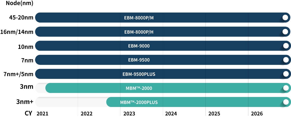
Development Roadmap
The multi-electron beam mask writer is a photo-mask writer for advanced technology nodes that controls 260,000 beams at high speed and high precision, enabling high-throughput and high-precision photomask manufacturing. Multi-EB Mask Writer "MBMTM-2000" is compatible with 3nm Node Design Rule. Multi-EB Mask Writer " MBM™-2000PLUS " is compatible with 3nm+ Node Design Rule.
The EB Mask Writer system series with variable electron beam, variable stage speed control and high current density enables low COO ( Cost of Ownership ). Variable EB Mask Writer system "EBM-9500PLUS" is compatible with 7nm+/5nm node. "EBM-9500" is compatible with 7nm node."EBM-9000" is compatible with 10nm node. Variable EB Mask Writer system "EBM-8000P/H, EBM-8000P/M" is compatible with 45~14nm node.
NuFlare Technology will continue to develop leading-edge mask writers while watching the trend of next generation lithography technology, such as EUV or nanoimprint, to meet the needs of developing devices for 2nm generations and after.